In this post I’ll be covering the process of getting the brains of my custom cartridge working; a Xilinx XC9572XL CPLD. Hang on to your hats.
First, let’s briefly talk about what a CPLD is. This chip is similar to an FPGA in that it provides the ability to reprogram its hardware, rather than running software. Unlike an FPGA, it has non-volatile memory, so the configuration will stay in the chip even after power is lost. The trade-off is that the amount of logic units is orders of magnitude smaller than an FPGA. Fortunately, this project is relatively simple, so I have no doubt it will fit within the limits of the chip. Unfortunately, I’ve never used a CPLD and my only experience with FPGAs was an intro logic class 7 years ago.
For this project we’ll be using the stable, light-weight, robust, intuitive and frequently updated software provided by Xilinx called Webpack ISE. What’s that? It’s a 6.5GB download split over four files? It requires an account to download a license? It’s laggy and confusing and was discontinued in 2013? Well hey, at least it’s free (and runs on Linux in addition to Windows).
For this project, I’m writing the code in Verilog, which is a Hardware Description Language that allows you to define the internal layout of the CPLD by writing code. The other popular choice is VHDL (which does not stand for “Verilog Hardware Description Language”, rather “VHSIC Hardware Description Language“, where VHSIC stands for “Very High Speed Integrated Circuit”… Sure, why not). If you’re hoping to learn Verilog from this blog post — don’t. I’m learning as I go and the code here is technically functional, but that’s about all you can say about it.
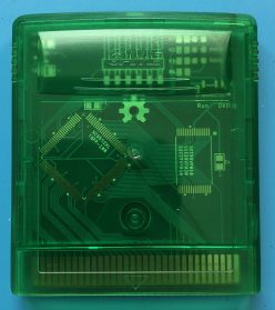
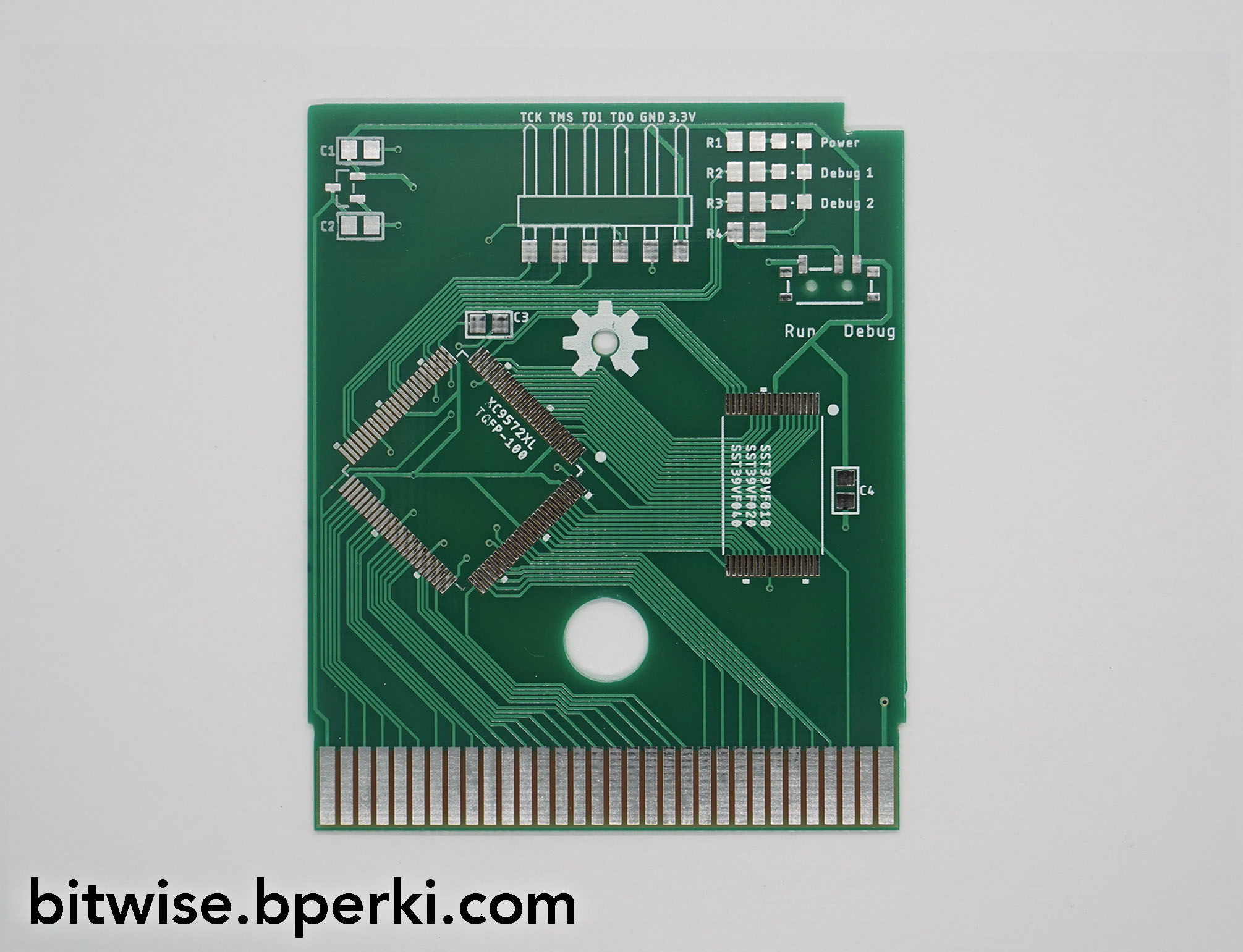
In my last post, I showed a development board for the XC9572XL I made that included three buttons and eight LEDs, as well as breaking out all of the pins. It was useful for debugging since I could access all of the pins, but for the sake of this blog post, all my examples are going to use the custom Game Boy Cartridge board. Although it only has 28 pins broken out, a single switch and two LEDs, it has the parallel flash chip on board, which is what I really needed. Hooking up 30 jumper wires between two breakout boards just wasn’t practical.
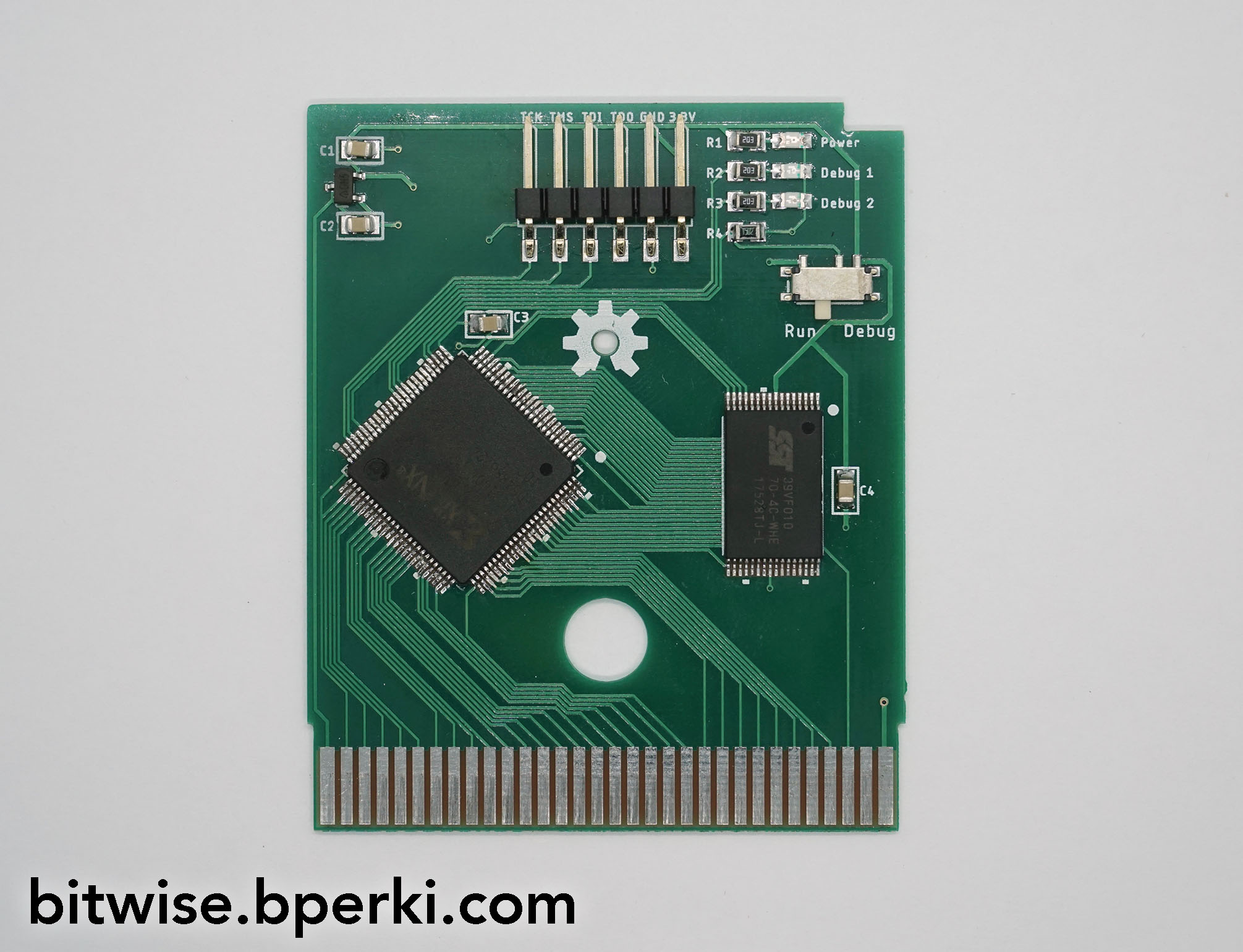
The first example is as simple as it gets. I define the switch as an input and the two LEDs as outputs and toggle the LEDs depending on the position of the switch (the actual pin definitions happen in a separate User Constraints File).
module GamePakHello(
	SWITCH, LED1, LED2
);
	input SWITCH;
	output LED1;
	output LED2;

	assign LED1 = SWITCH;
	assign LED2 = !SWITCH;
endmodule
Now that we have some Verilog that synthesizes (sort of like the hardware equivalent of “compiling”), how do we go about getting it on our chip? For this, we need to generate an XSVF file, which contains a compressed list of instructions that tell the CPLD how it should configure its internal hardware. To use this file, we need an XSVF player, which interprets the commands and sends them over the JTAG interface to our chip. One of the goals I had for this project was to make it easy for anyone to replicate, so I wanted to stay away from expensive tools and software when possible. There are lots of possibilities to accomplish this (UrJTAG supports many cheap JTAG devices), but I didn’t have any of those around, so I decided to use this library, which allowed me to use any old Arduino to flash my CPLD — thanks mrjimenez! The library comes with an example sketch that includes everything you need to get started; I downloaded it to my Arduino, hooked up the JTAG pins (TCK, TMS, TDI, and TDO) on my cartridge to the specified Arduino pins and ran the companion Python program.
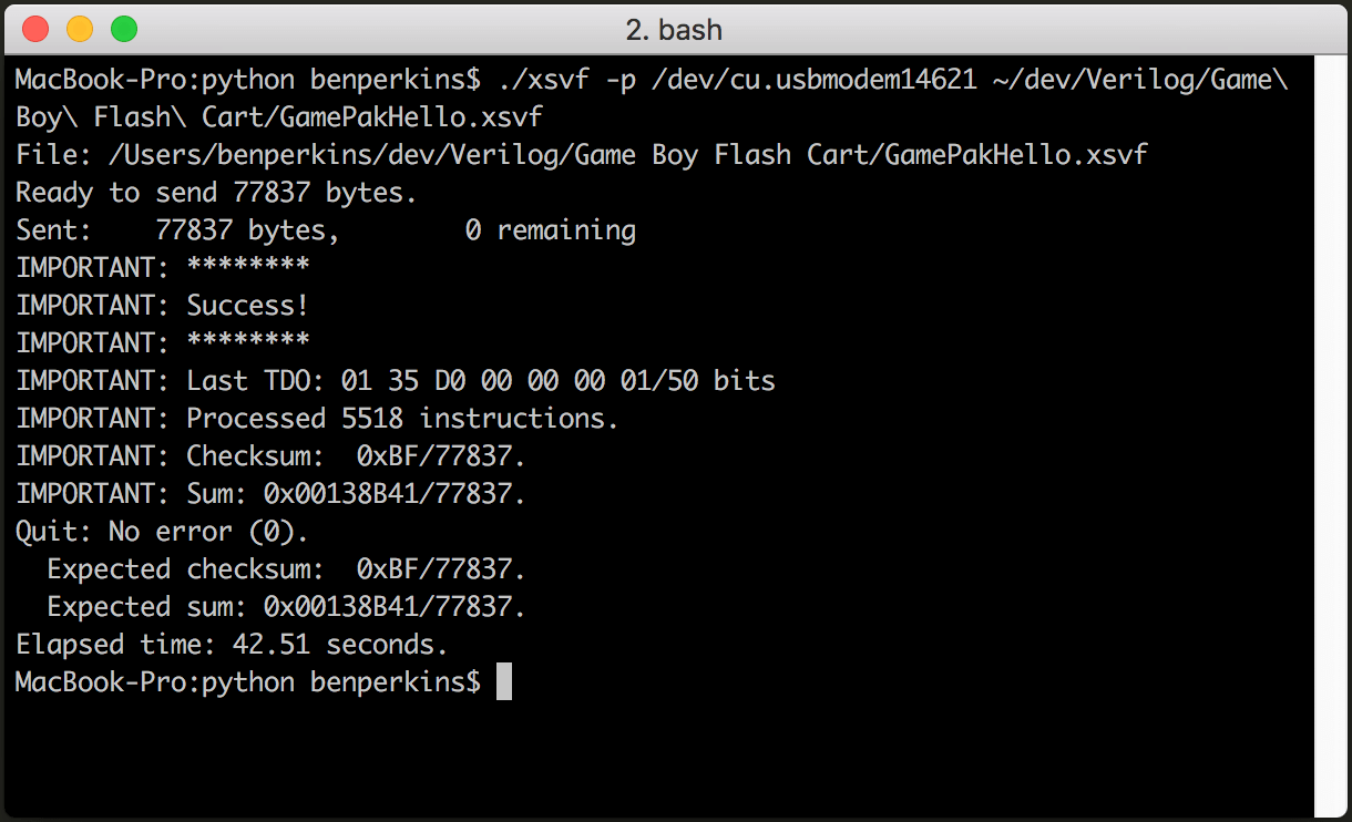
Playing the XSVF files to configure the CPLD is easy; clone the JTAG XSVF Player into your Arduino Libraries directory, flash the example to an Arduino, then navigate to the extras/python subdirectory in a terminal window and run:
./xsvf -p (Arduino Serial Port) (Path To XSVF)
In my case:
./xsvf -p /dev/cu.usbmodem14621 ~/dev/verilog/GameBoyFlashCart/GamePakHello.xsvf
The next example shows how to blink the LEDs without any external clock. This CPLD has no internal clock circuitry — the Game Boy will eventually provide a 1MHz clock signal — so we’re going to take advantage of the natural propagation delay in the logic elements to create a rough clock. This technique really shouldn’t be used for anything other than “eh, just wait a bit” sort of timing, since it will vary from chip to chip and with temperature. It can even vary inside the chip itself — that is, if two different parts of this design were looking at this clock, they may see signals slightly shifted from one another as the clock signal propagates throughout the chip. This is irrelevant for the purpose of this example, though. Here we use our pseudo-clock signal to drive a counter, and we use the counter to toggle the LEDs. Depending on the state of the switch, the first LED will toggle every time the 24th or 25th bit changes state (every 16,777,216 or 33,554,432 cycles) and the second LED will toggle with the 26th or 27th bit (67,108,864 or 134,217,728 cycles).
module GamePakHello(
	SWITCH, LED1, LED2
);
	input SWITCH;
	output LED1;
	output LED2;
	output CLK;

	wire CLK;
	assign CLK = !CLK;
	reg [31:0] timer = 32'b0;
	reg state;

	assign LED1 = SWITCH ? timer[25] : timer[24];
	assign LED2 = SWITCH ? timer[27] : timer[26];

	always @(posedge CLK) begin
		timer <= timer + 1;
	end
endmodule
Ok, so… 1000 words into this post and all I’ve done is blink some LEDs? Let’s kick it up a notch and see if we can say hi to the Game Boy:
module GameBoyTest(
  CLK, RD, WR, CS, A, D
);

  // Inputs
  input CLK;
  input RD;
  input WR;
  input CS;
  input [15:0] A;
  // Outputs
  output [7:0] D;

  // Registers
  reg [7:0] data;

  assign D = data;

  // Whenever Game Boy clock goes low
  always @ (negedge CLK)
  begin
    case (A)
      16'h0104 : data <= 8'hCE;
      16'h0105 : data <= 8'hED;
      16'h0106 : data <= 8'h66;
      16'h0107 : data <= 8'h66;
      16'h0108 : data <= 8'hCC;
      16'h0109 : data <= 8'h0D;
      16'h010A : data <= 8'h00;
      16'h010B : data <= 8'h0B;
      16'h010C : data <= 8'h03;
      16'h010D : data <= 8'h73;
      16'h010E : data <= 8'h00;
      16'h010F : data <= 8'h83;
      16'h0110 : data <= 8'h00;
      16'h0111 : data <= 8'h0C;
      16'h0112 : data <= 8'h00;
      16'h0113 : data <= 8'h0D;
      16'h0114 : data <= 8'h00;
      16'h0115 : data <= 8'h08;
      16'h0116 : data <= 8'h11;
      16'h0117 : data <= 8'h1F;
      16'h0118 : data <= 8'h88;
      16'h0119 : data <= 8'h89;
      16'h011A : data <= 8'h00;
      16'h011B : data <= 8'h0E;
      16'h011C : data <= 8'hDC;
      16'h011D : data <= 8'hCC;
      16'h011E : data <= 8'h6E;
      16'h011F : data <= 8'hE6;
      16'h0120 : data <= 8'hDD;
      16'h0121 : data <= 8'hDD;
      16'h0122 : data <= 8'hD9;
      16'h0123 : data <= 8'h99;
      16'h0124 : data <= 8'hBB;
      16'h0125 : data <= 8'hBB;
      16'h0126 : data <= 8'h67;
      16'h0127 : data <= 8'h63;
      16'h0128 : data <= 8'h6E;
      16'h0129 : data <= 8'h0E;
      16'h012A : data <= 8'hEC;
      16'h012B : data <= 8'hCC;
      16'h012C : data <= 8'hDD;
      16'h012D : data <= 8'hDC;
      16'h012E : data <= 8'h99;
      16'h012F : data <= 8'h9F;
      16'h0130 : data <= 8'hBB;
      16'h0131 : data <= 8'hB9;
      16'h0132 : data <= 8'h33;
      16'h0133 : data <= 8'h3E;
      default : data <= 8'h0;
    endcase
  end
endmodule
Any guesses what the above code does? For those who aren’t familiar with the Game Boy, the first thing that it does when it boots is read a specific section of memory from the cartridge and draws it to the screen. This memory (0x104 to 0x133) contains the Nintendo logo that scrolls down from the top of the screen when the Game Boy powers up. If any bit is different from what the Game Boy expects, the system locks up.
The above Verilog allows us to send this logo to the Game Boy, let’s step through to find out how. First, I define the clock (CLK), read (RD), write (WR), chip select (CS) and address (A) as inputs, and I define data (D) as an output. For simplicity, we can ignore all of the signals except for CLK, A and D. CLK tells us when we need to provide new data and A tells us what data to provide. Each time the clock signal goes low, we check what address the Game Boy is requesting and if it falls within the range 0x104 to 0x133, we use our lookup table to set the data bus to the correct byte. Any other address is ignored by setting 0 on the data bus (0x00 is the nop op-code, which tells the Game Boy to do nothing after drawing the logo).
That’s all there is to it! In my next post, I’ll talk about parallel flash and load a fully functional game onto the cartridge! Stick around.